Rapid design cycles and tighter BOM timelines are driving engineers and purchasers to rely on ready-to-download datasheets. Having the 1838266-3 datasheet available at design time reduces procurement risk, shortens validation loops, and helps teams verify thermal and EMI margins before prototype spin. This article supplies a full-spec breakdown, clear pinout explanation, and practical steps to obtain and verify a safe PDF for hardware engineers, purchasers, and PCB designers.
1 — Background: Quick overview of the 1838266-3
1.1 Device family & primary function
The 1838266-3 is a board-mount connector class device intended for signal and low-power distribution in embedded systems. Common applications include industrial controllers, telemetry modules, and modular I/O assemblies where reliable mating, retention, and predictable impedance matter. Presenting concise specifications helps readers decide fit-for-purpose quickly while establishing the component’s system-level role.
1.2 Key specs at a glance (summary card)
At a glance, this compact summary maps the physical and environmental boundaries of the 1838266-3. It primes hardware development teams with the absolute vital values required during the preliminary component selection phase:
| Key Parameter | Specification Profile |
|---|---|
| Connector Style | M12, A-Coded, 5 Positions, Male Pin |
| Mounting Configuration | Right Angle, Through-Hole Board Mount (THT) |
| Current Rating | 4.0 A per Contact (Continuous) |
| Voltage Rating | 60.0 V AC / DC |
| Operating Temp Range | -25°C to +85°C |
| Ingress Protection | IP67 (When fully mated and locked) |
2 — Full electrical and performance specifications (data deep-dive)
2.1 Electrical ratings: voltages, currents, power & limits
To secure a reliable design inside safety-critical industrial loops, layout designers and power analysts must adhere to absolute limits. The table below details the electrical parameters, safety factors, and test conditions defined by the manufacturer:
| Parameter | Symbol | Min | Typ | Max | Units | Test Conditions |
|---|---|---|---|---|---|---|
| Rated Operational Voltage | VOP | — | — | 60 | V | IEC 60664-1 Pollution Degree 3 |
| Rated Current (All poles loaded) | IR | — | — | 4.0 | A | Ambient Temp = 40°C |
| Contact Resistance | RC | — | — | 10.0 | mΩ | IEC 60512-2-1, initial |
| Insulation Resistance | RINS | 100 | — | — | MΩ | IEC 60512-3-1, 500 VDC test |
| Dielectric Withstanding Voltage | VDW | 1000 | — | — | VAC | 1 minute duration, sea level |
2.2 Dynamic / timing / performance characteristics
Electrical performance extends beyond steady-state constraints. In transient, signal-carrying environments, the connector interface exhibits passive behavior that layout engineers must balance. Contact bounce during physical mating cycles can inject high-frequency transients into delicate transceiver inputs; thus, external signal conditioning or ESD suppression is advised. The insertion impedance remains negligible at standard industrial bus speeds (such as CAN, RS-485, and industrial Ethernet up to 10 MHz), but impedance matching must be verified when approaching higher frequencies.
3 — Pinout, package and mechanical details
3.1 Pinout diagram and pin descriptions
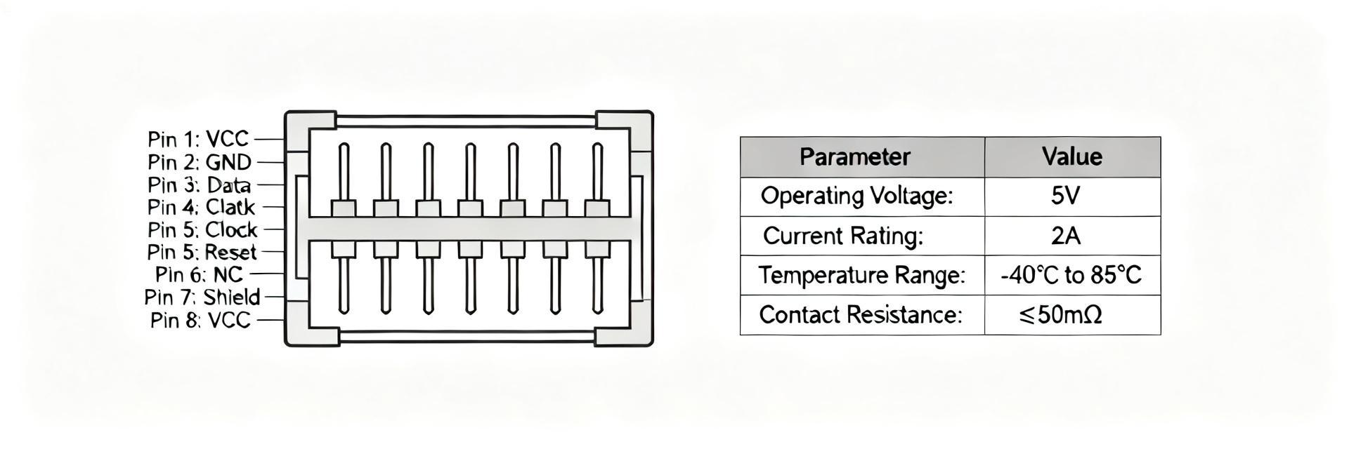
The standard A-coded 5-pin configuration is mapped to prevent wiring errors. Signal lines must correspond closely to standard industrial sensor/actuator cabling conventions (such as IEC 61076-2-101):
| Pin Number | Standard Name | Type | Industrial Function / Connection |
|---|---|---|---|
| Pin 1 | L+ / VCC | Power | Positive Supply Voltage (+24VDC Typical) |
| Pin 2 | I/O / OUT2 | Signal | Auxiliary Digital Output / Secondary Signal |
| Pin 3 | L- / GND | Power | System Power Ground / Common Return |
| Pin 4 | OUT1 / C/Q | Signal | Primary Switching Output / IO-Link Comms |
| Pin 5 | Shield / FE | Shield | Functional Earth / Chassis Ground Connection |
3.2 Package drawings, footprint and mechanical tolerances
The 1838266-3 features a right-angle profile designed to mount directly to the edge of standard 1.6mm or 2.4mm thick PCBs. The housing holds an integrated metal thread shell which links with the panel cutout for grounding. Footprint configurations must provide 1.2mm through-holes for the signal contacts and 2.5mm anchor holes for the structural/ground shielding tabs to withstand mechanical mating stresses without straining raw solder joints.
4 — How to download and verify the 1838266-3 datasheet PDF safely
4.1 Where to obtain the PDF and how to verify authenticity
To avoid counterfeit parts and design errors stemming from obsolete data, prioritize the engineering documentation pipeline as follows:
- Primary Source: TE Connectivity's official part detail portal.
- Secondary Source: Authorized global industrial distributors (e.g., Mouser, DigiKey, Arrow) with real-time API-driven document linkages.
- Document Integrity Checklist:
- Verify the SHA-256 checksum of the downloaded document file.
- Ensure the document contains the exact revision code matching the manufacturer's global change notification (PCN) registry.
- Confirm high-resolution vector schematic assets that remain sharp at extreme zoom levels, which is standard for native CAD integration.
4.2 How to extract the pinout/specs from the PDF efficiently
When porting values into ECAD software like Altium Designer, OrCAD, or KiCad, run a strict verification pass. Use PDF text search to index standard key parameters such as "1838266", "A-coding", and "contact arrangement". If integrating the physical footprint from a vector drawing, export the scaling metadata explicitly in millimeters rather than imperial units to eliminate rounding drift across the 5-pin layout grid.
5 — Practical design checklist & application guidance
5.1 Schematic & PCB layout best practices (pinout-driven)
A successful design hinges on careful PCB layout and routing. Use the following pinout-driven guidelines:
- Impedance and Separation: Route signal paths (Pins 2 and 4) away from switched power channels to prevent cross-coupling.
- Shield Grounding: Connect the shield anchor pin (Pin 5/Housing) to your system chassis ground via a low-impedance copper plane. Incorporate a parallel RC network (typically 1 MΩ || 4.7 nF / 2 kV) if galvanic isolation is required.
- ESD Protection: Place TVS diode arrays near the physical connector pins before they enter any high-density controller IC paths.
5.2 Thermal management, derating and test checklist (specifications-driven)
The maximum current rating of 4.0A is strictly derated when operating close to environmental limits. At 80°C, the continuous current capacity must be restricted to 2.5A per contact to maintain the maximum internal terminal junction temperature below +85°C. When validating prototypes, use thermal imaging cameras to inspect current-carrying traces during load testing to confirm your trace width calculations provide a safe thermal margin.
Summary
- Keep a verified 1838266-3 datasheet in the component library to accelerate BOM decisions; ensure checksum and revision metadata are recorded with the file for traceability and compliance.
- Prioritize the pinout and package callouts during schematic capture: mapping pin functions and footprint tolerances prevents late-stage layout rework and enclosure interference.
- Derate using published thermal and current specifications, and run targeted bench tests to validate margins under worst-case conditions before production runs.
Frequently Asked Questions
How can I confirm the correct revision of the 1838266-3 datasheet?
Open the PDF properties to check revision or version fields, then compare the revision string and document change log (if present) against your internal component record. Verify that figures and table contents match expected test conditions; if in doubt, obtain an official confirmation from the manufacturer channel or authorized distributor.
What if pin numbers differ between package options for the 1838266-3?
Compare package drawings side-by-side and create a mapping table linking alternative package pin numbers to canonical signal names. Update schematic symbols and footprint libraries with package variant identifiers to avoid mis-mating or incorrect net assignments during PCB fabrication and assembly.
Should I rely on typical vs. maximum values in the specifications?
Design to recommended operating and maximum limits, not typical values. Typical figures are for reference and performance expectations; use max/min ratings for margin calculations and worst-case testing to ensure reliability across manufacturing and environmental variation.


